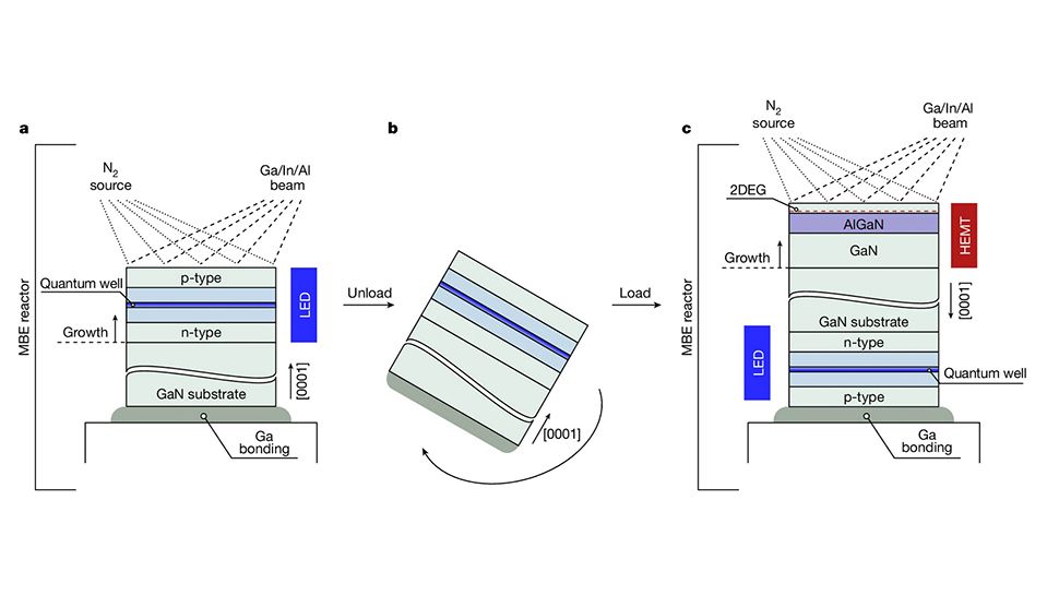
Researchers at Cornell University, in collaboration with the Polish Academy of Sciences, have made a major breakthrough in semiconductor technology by developing the first-ever dual-sided chip – referred to as a “dualtronic” chip – that integrates both photonic and electronic devices on a single Gallium Nitride (GaN) wafer.
This innovation could shrink device sizes, improve energy efficiency, and reduce manufacturing costs.
The GaN wafer’s unique crystal structure is key to its dual functionality. Each side of the wafer has different properties, similar to how the poles of a magnet differ. The team utilized the metal-polar (Ga-polar) side to create light-emitting diodes (LEDs) and the nitrogen-polar (N-polar) side to construct high-electron mobility transistors (HEMTs). By doing so, they were able to achieve a configuration where the HEMT on one side powers the LED on the other – an accomplishment never before realized in any semiconductor material.
Limited only by the imagination
The research, led by Cornell professors Debdeep Jena and Huili Grace Xing, along with co-lead authors Len van Deurzen and Eungkyun Kim, has been published in the Nature journal.
“To our knowledge, nobody has made active devices on both sides, not even for silicon,” noted co-lead author Len van Deurzen, emphasizing how this feat was possible only because of GaN’s polarity-dependent properties. Traditional silicon wafers are cubic, making both sides nearly identical, which prevents such a design.
According to the researchers, this dualtronic approach could have immediate applications in making microLED displays more affordable and energy-efficient. By integrating photonic and electronic functions into a single chip, fewer components would be needed, leading to lower production costs and a smaller device footprint. This advancement could significantly impact display manufacturing, potentially making LED displays cheaper and more compact.
The technology’s potential goes even further. With the ability to use the same wafer for different functions, dualtronics could enable smartphone screens to be repurposed as antennas, supporting wireless communications directly through the display. The polarization properties of GaN and the dualtronic chip’s multifunctionality could transform not only displays but also radio frequency devices, lasers, and future 5G/6G technologies.
“A good analogy is the iPhone,” explained Debdeep Jena. “It is, of course, a phone, but it is so many other things. It’s a calculator, it’s a map, it lets you check the internet. So there’s a bit of a convergence aspect of it. I would say our first demonstration of ‘dualtronics’ in this paper is convergence of maybe two or three functionalities, but really it’s bigger than that.”
This breakthrough could reshape how semiconductor devices are designed and utilized. By eliminating the need for separate chips to handle different functions, dualtronics promises to optimize both performance and resource utilization across a variety of technologies. As the researchers point out, this development marks a significant step forward, and the potential applications are “limited only by the imagination.”
More from TechRadar Pro
Services Marketplace – Listings, Bookings & Reviews
