SK Hynix, one of the biggest rivals to Samsung, has been making some major announcements recently, including plans to construct the world’s largest chip factory, and a tie up with TSMC to produce the next-generation of High Bandwidth Memory, known as HBM4.
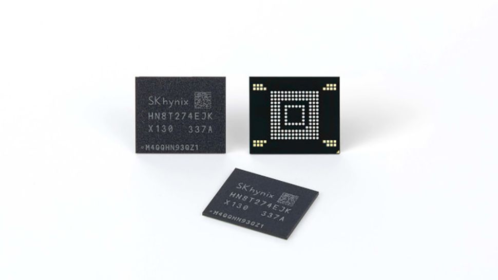
The company’s latest move is the development of a next-generation mobile NAND solution called Zoned UFS (ZUFS) 4.0, which is optimized for on-device AI in mobile devices, particularly smartphones.
ZUFS technology classifies and stores data generated from smartphones in different zones, based on their characteristics. In contrast to a traditional UFS, ZUFS 4.0 groups and stores data with similar purposes and frequencies, which reportedly boosts the speed of the device’s OS and improves overall storage efficiency.
ZUFS production
SK Hynix claims “The ZUFS also shortens the time required to run an application from a smartphone in long hours use by 45%, compared with a conventional UFS. With the issue of degradation of read and write performance improved by more than four times, the lifetime of the product also increased by 40%.”
SK Hynix says ZUFS 4.0 meets JEDEC specifications and that mass production of the chip will begin in the third quarter.
Ahn Hyun, the Head of the N-S Committee at SK Hynix, stated that customers are demanding higher quality memory solutions as major tech firms shift their focus towards developing on-device products that incorporate their own generative AI applications. He said the company will “continue to work toward strengthening its leadership as the global top AI memory provider by supplying high-performance NAND solutions that meet such higher requirements at a right time, while building up stronger partnership with leading ICT companies.”
More from TechRadar Pro
Services Marketplace – Listings, Bookings & Reviews